(China (Mainland))


Product Summary
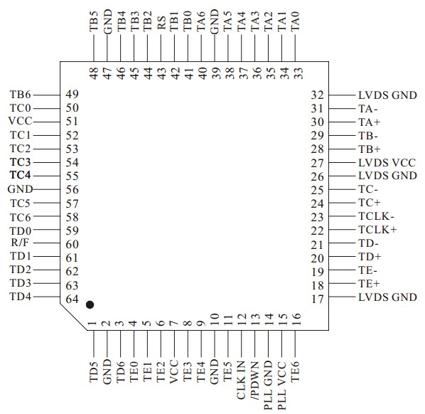
The THC63LVD103 transmitter is designed to support pixel data transmission between Host and Flat Panel Display from NTSC up to SXGA+ resolutions. The THC63LVD103 converts 35bits of CMOS/TTL data into LVDS(Low Voltage Differential Signaling) data stream. The THC63LVD103 transmitter can be programmed for rising edge or falling edge clocks through a dedicated pin. At a transmit clock frequency of 135MHz, 30bits of RGB data and 5 bits of timing and control data (HSYNC, VSYNC, DE, CNTL1, CNTL2) are transmitted at an effective rate of 945Mbps per LVDS channel.
Parametrics
THC63LVD103 absolute maximum ratings: (1)Supply Voltage (VCC) : -0.3V to +4.0V; (2)CMOS/TTL Input Voltage: -0.3V to (VCC + 0.3V); (3)CMOS/TTL Output Voltage: -0.3V to (VCC + 0.3V); (4)LVDS Driver Output Voltage: -0.3V to (VCC + 0.3V); (5)Junction Temperature: +125°C; (6)Storage Temperature Range: -55°C to +150°C; (7)Resistance to soldering heat: +260°C /10sec; (8)Maximum Power Dissipation @+25°C: 1.0W.
Features
THC63LVD103 features: (1)Wide dot clock range: 8-135MHz suited for NTSC, VGA, SVGA, XGA,SXGA and SXGA+ ; (2)PLL requires no external components; (3)Supports spread spectrum clock generator; (4)On chip jitter filtering ; (5)Clock edge selectable; (6)Supports reduced swing LVDS for low EMI; (7)Power down mode; (8)Low power single 3.3V CMOS design; (9)64pin TQFP; (10)Backward compatible with THC63LVDM63R(18bits) / M83R(24bits).
Diagrams
| Image | Part No | Mfg | Description |  |
Pricing (USD) |
Quantity | ||||
|---|---|---|---|---|---|---|---|---|---|---|
 |
 THC63LVD103 |
Other |
|
Data Sheet |
Negotiable |
|
||||
| Image | Part No | Mfg | Description | |
Pricing (USD) |
Quantity | ||||
|
THC63LVD103 |
Other |
|
Data Sheet |
Negotiable |
|
||||
|
THC63LVD104A |
Other |
|
Data Sheet |
Negotiable |
|
||||
|
THC63LVD104S |
Other |
|
Data Sheet |
Negotiable |
|
||||
|
THC63LVD823 |
Other |
|
Data Sheet |
Negotiable |
|
||||
|
THC63LVD824 |
Other |
|
Data Sheet |
Negotiable |
|
||||
|
THC63LVDF64A |
Other |
|
Data Sheet |
Negotiable |
|
||||